
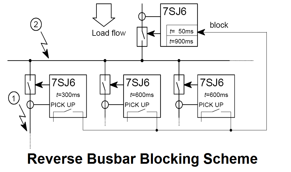
The reverse busbar protection is a cost-effective solution for the accelerated clearance of busbar faults in distribution systems. It can only be applied on single busbars with a fixed direction of power flow and fault current flow. In picture 3, a typical application is shown.

Overview:
For this application, the protection device on the incoming bay (usually the transformer bay) will be provided with blocking signals from the outgoing bays (the feeder bays). If one of the outgoing bays (feeder bays) detects a fault, (pick-up signal), this bay must route a blocking signal to protect the incoming bay. This blocking signal prevents the fast tripping of the incoming bay (I>> stage). The block signal may only be present for one second.
For this application, a CFC chart in the incoming bay is required. Although it is possible to allocate a signal from a binary input so that it provides the blocking of a protection stage it is not possible to give more than one binary input to directly block one protection stage (the reason being that if two binary inputs that provide the same blocking signal have a different state, the device logic would not know which of the two binary inputs should be used).


Example application with 7SJ6 relays:
The I>> stage in the in-comer will be blocked with the signal 1721 >Block 50-2., and the signal 1724 >Block 50N-2. These signals must be allocated with source CFC. (see picture 1)

Picture 1: input/output matrix in the incoming bay relay

For example, a feeder relay (or many feeder relays with a blocking signal connected in parallel) designated as LHBB-block provides a blocking input signal via binary input to the incoming bay relay. This signal is routed to the user-defined single-point annunciation in the matrix (picture 1), binary input 20. Similarly, the second feeder relay (or second group of relays) designated as RHBB-block is/are allocated to binary input 21. Two new user-defined single-point annunciations, which have to be connected to the binary inputs must be generated. These signals (in picture 1) are called LHBB-Block and RHBBBlock. These signals must be routed with the destination CFC so that they will be available inside the CFC charts. In the CFC chart, the LHBB-Block and RHBB-Block signals are connected via OR-gate. The output of the OR gate triggers a timer that restricts the blocking signal to one second. This is achieved by applying the timer output via a negator to an AND gate (AND gate 4 in picture 2). The timer output will change from 0 to 1 one second after the OR gate output changes to 1. At this point, the second input of AND gate 4 will change to 0, thereby removing the blocking signal which is routed from OR gate one via the AND gate to the right-hand margin. As shown in picture 2, the blocking signal from the CFC chart is derived from the output of the AND gate and is routed to the signals 1721 >Block 50-2. and 1724 >Block 50N-2. Please note that the gates must be executed in the correct sequence, i.e. sequences 10 to 13 as shown in picture 2. The sequence of execution may commence with a different
number, depending on other logic located in the same execution layer, PLC_BEARB). The OR gates must be first in the sequence, followed by the timer, negator, and AND gate in turn.

Picture 2: CFC chart to implement the blocking in the incoming bay

Picture 3: typical reverse busbar scheme

Our Completed Courses: